2022
Nixie tubes, or cold cathode display tubes, are a vintage electronic device that can be used to display information, typically numbers. They were widely used in displays and indicators throughout the 20th century. Nowadays, they are rather hard to come by, but some hobbyists still like to use them in projects. A common use of them now, is to create nixie tube clocks – a digital clock that uses nixie tubes to display the clock digits.


About a year ago, I bought six nixie tubes off eBay with this project in mind, but I never got around to it, until autumn 2022, when I decided to finally get on with it. This was my first project that involved using a discrete microcontroller chip (that is, not one on a breakout, like the Arduino, or similar).
- Introduction to Nixie Tubes
- Driving Nixie Tubes
- Digit Separators & Coloured LEDs
- Microcontroller & Digital Logic
- Real Time Clock with I2C
- Power Supplies
- PCB Design & Construction
- Programming
- Final Result
Introduction to Nixie Tubes
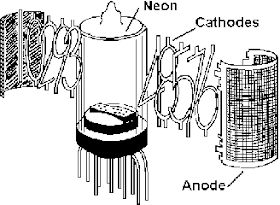
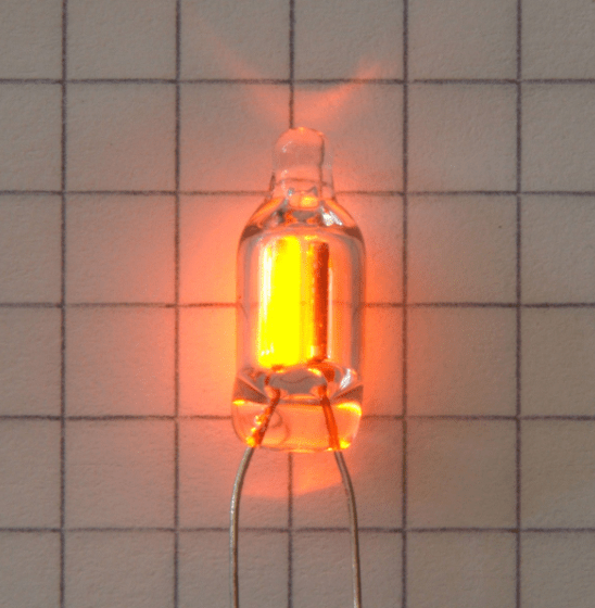
But how do nixie tubes work? It is quite similar to a neon lamp. I used dual-neon lamps for my digit separators (colons). Neon lamps are a glass container, containing neon gas, and with two electrodes inside. A relatively high voltage is applied to the electrodes (around 100V) to cause them to illuminate. Nixie tubes function similarly, as they are also composed of electrodes within an evacuated class container, which is filled with low pressure neon gas. However, unlike the basic neon lamp, nixie tubes typically have ten cathodes, shaped like the digits from 0 to 9, and a single anode, in the form of a sort of “cage” around the cathodes. By allowing current to flow through one of the cathodes, we cause it to be illuminated.
Nixie tubes typically require a voltage of around 180V to be applied between the anode and a cathode for them to work. This causes a strong electric field to develop between the cathode and the anode. This can ionise the gas molecules around the cathode, causing electrons in the neon atoms to be excited. As the electrons change energy level, they emit light. Neon atoms happen to emit orange photons, but if a different gas was used, the digits would illuminate with a different colour.
The voltage necessary for the nixie tube to start glowing is called the striking voltage. Once this voltage, typically around 180V, is reached, the voltage drops to the sustain voltage, which is around 140V. Nixie tubes behave in a manner similar to an LED, as they must be current limited to stop damage occurring. This is usually done with a series resistor connected to the anode. Typical safe current values are around 1-3mA. If the nixie tube is not properly current limited, it will degrade quickly, possibly even dying as soon as it is turned on, if your power supply can supply amps of current.
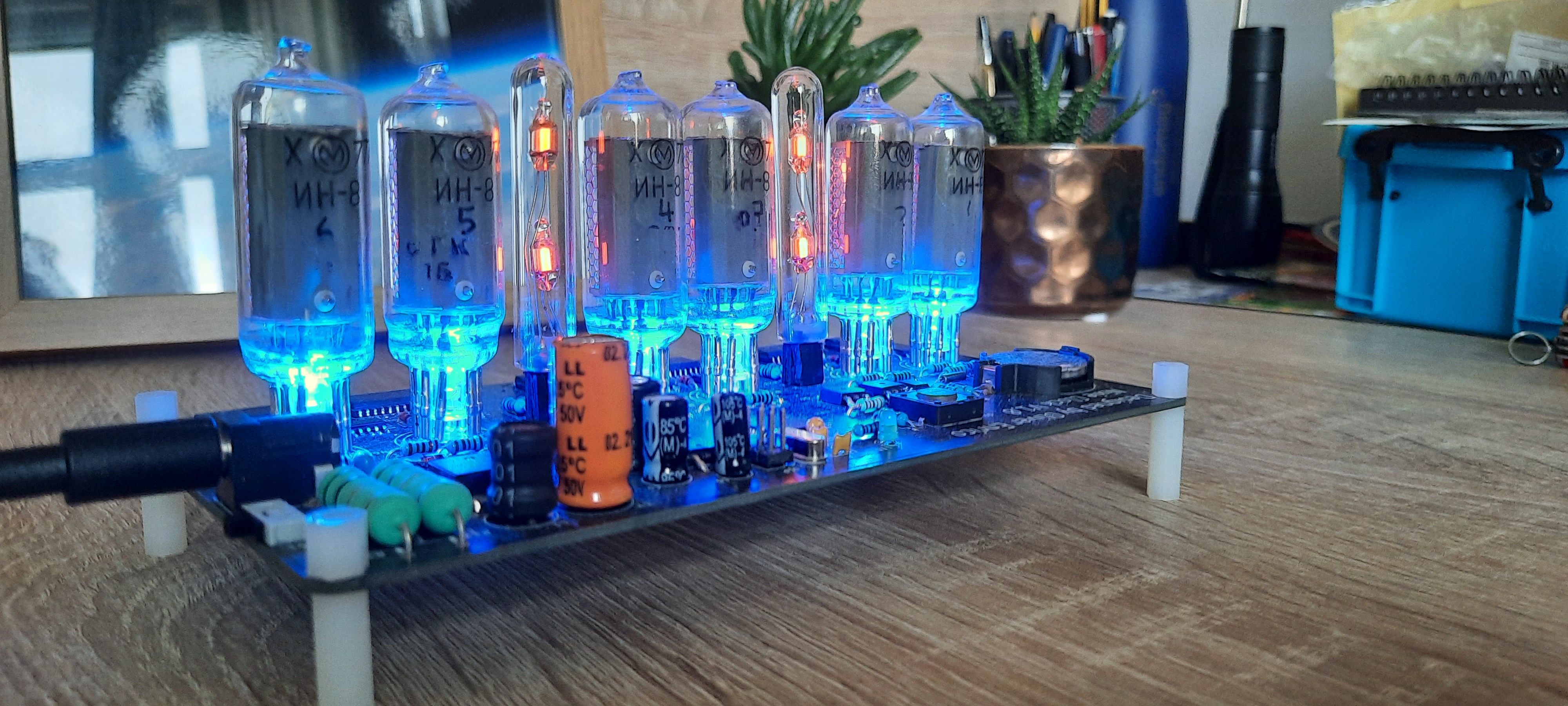
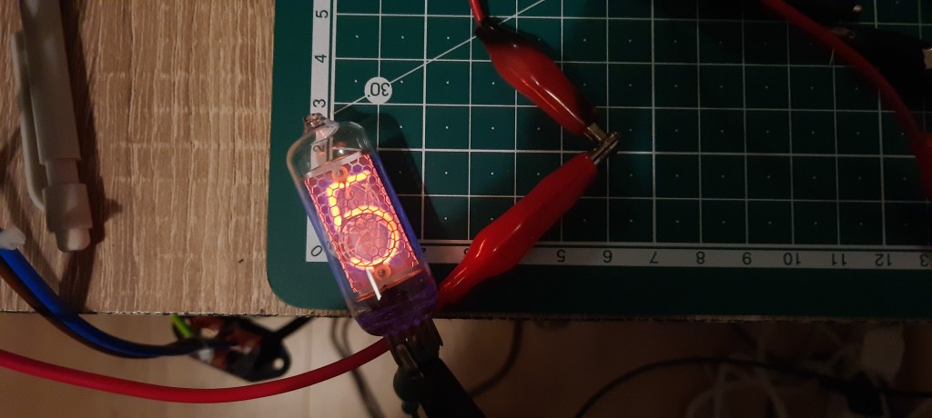
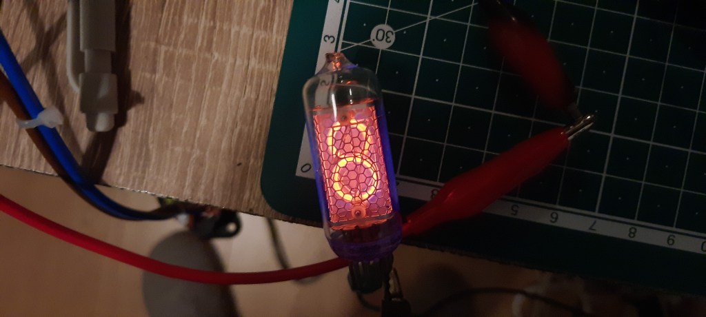
The first task was to try getting the tubes I had to illuminate, to both confirm that they were working, and that I could drive them properly. I cobbled together a high voltage power supply from one of my exploded tesla coil driver boards, on which the mains rectifier was still working. Using this, I was able to attach crocodile clips to the pins of my nixie tubes. I included a 33kΩ series resistor to limit the current through the tube. To my delight, all the tubes worked just fine!
Driving Nixie Tubes
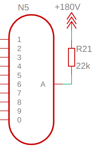
Whilst making a single digit on one tube illuminate was quite exciting, the final clock needed six tubes, displaying 10 digits, all controlled by some electronics. So I had to come up with some way to turn the digits on and off without connecting a crocodile clip to its respective pin on the base. The 180V supply is connected to the single anode of each tube, and we can insert the current limiting resistor here, so that only one is needed per tube, rather than 10. To turn on a digit, we will need to connect the relevant cathode pin to ground using some circuit.
I was planning to control the whole clock with a ATmega microcontroller, and it certainly would not be suitable for switching the 180V signals directly. I think you used to be able to get special ICs that were designed for controlling nixie tubes, but as no one uses them anymore, the ICs are no longer manufactured, and are hard to get your hands on. Not to worry though, as it is actually quite simple to drive them. We can simply connect a transistor from each cathode pin to ground, and connect the microcontroller to the base of the transistor.
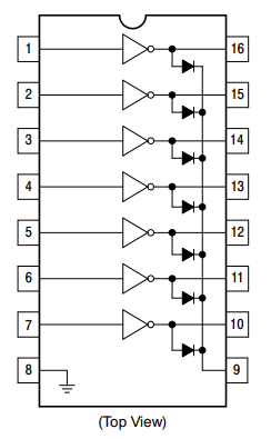
If we were to use discrete transistors, this would require at least 60 of them on the board! If we went for a Darlington pair configuration, we would need 120! A more elegant solution is to use a transistor array, contained in a single IC. The ULN2003A from ON Semiconductor is an ideal candidate for the job! It is a 16-pin IC, which contains 7 NPN Darlington pairs. Integrated series input resistors, and internal suppression diodes are also nice bonuses!
The eagle-eyed among the readers of this may have noticed that the maximum voltage the transistors in the ULN2003A are rated for is only 50V. Yet we are using a 180V supply. So why can we use them? Well first of all, when a digit is turned on, the voltage of the cathode is pretty much at zero (plus whatever is lost in the transistor). All the voltage is lost across the nixie tube and the current-limit resistor. However, what is the voltage on the cathode pins when one is turned off? This is hard to say exactly, and varies wildly between tubes, and between different cathodes on the same tube, ranging from 20V to 120V. Voltages higher than the 50V maximum could cause damage to our driver.
Fortunately, the ULN2003A comes with diodes on the output of each driver, all connected to a common cathode. One way that others have got around the voltage issue, is to connect a Zener diode to the common cathode of the diodes, clamping the voltage on the output of the transistor drivers to below 50V. I decided to use the BZX79-C43 Zener diode, which had a Zener voltage of 43V. This should adequately protect the ULN2003A drivers. It is also important to check that this Zener is not conducting large amounts of current, which could potentially make the desired digit dim, or even illuminate other digits! Fortunately, Dave from the EEVblog tested this on his video about driving nixie tubes, and the diode does not affect the operation of the tube. This whole driver solution is based on Dave’s one, so check out his video for a more detailed explanation.
Digit Separators & Coloured LEDs
I wanted my clock to include something to clearly separate the pairs of tubes for the hours, minutes and seconds, as I thought it would look better with that. A common way this is done is to include a colon (:), like you might find on a normal digital clock. I didn’t have any nixie tubes with a colon-shaped cathode, but you can get dual-neon bulbs, that produce very similar-looking light, which would fit very nicely in.
Essentially, it is two independent neon lamps, stacked vertically in a glass tube. Neon lamps function the same way that nixie tubes do. To be honest, nixie tubes are just a special type of neon lamp. Driving the neon lamps is done in a very similar way to the nixie tubes, but discrete high voltage transistors were used instead of the ULN2003A Darlington array ICs. I used 100kΩ as the current-limiting resistor, with 33kΩ resistors feeding the bases of my FJD5304 NPN transistors that I was using the driver the lamps. I chose this transistor, as it has a maximum VCE of 400V! No need for any faffing around with Zener diode clamps with this!
It is also fairly common to put blue LEDs underneath the nixie tubes. When turned on, the light diffuses through the glass tube, giving a nice blue colour to the whole tube, which complements the orange digit very well. I wanted to included these on my design, but have them optionally turned on. That way, if I didn’t like the look of them in the end, I could simply turn them off. I elected to control them with the microcontroller that would be controlling the whole clock, and devised a circuit which used a single transistor to turn on all of the LEDs at one, while ensuring that they all had the same brightness.
Below you can see the schematic for the LED control circuit, as well as the schematic for the two pairs of neon lamps used as digit separators, with their driver circuits. The nets labelled “COLON_1” and “COLON_2” are connected directly to the microcontroller pins.

Microcontroller & Digital Logic
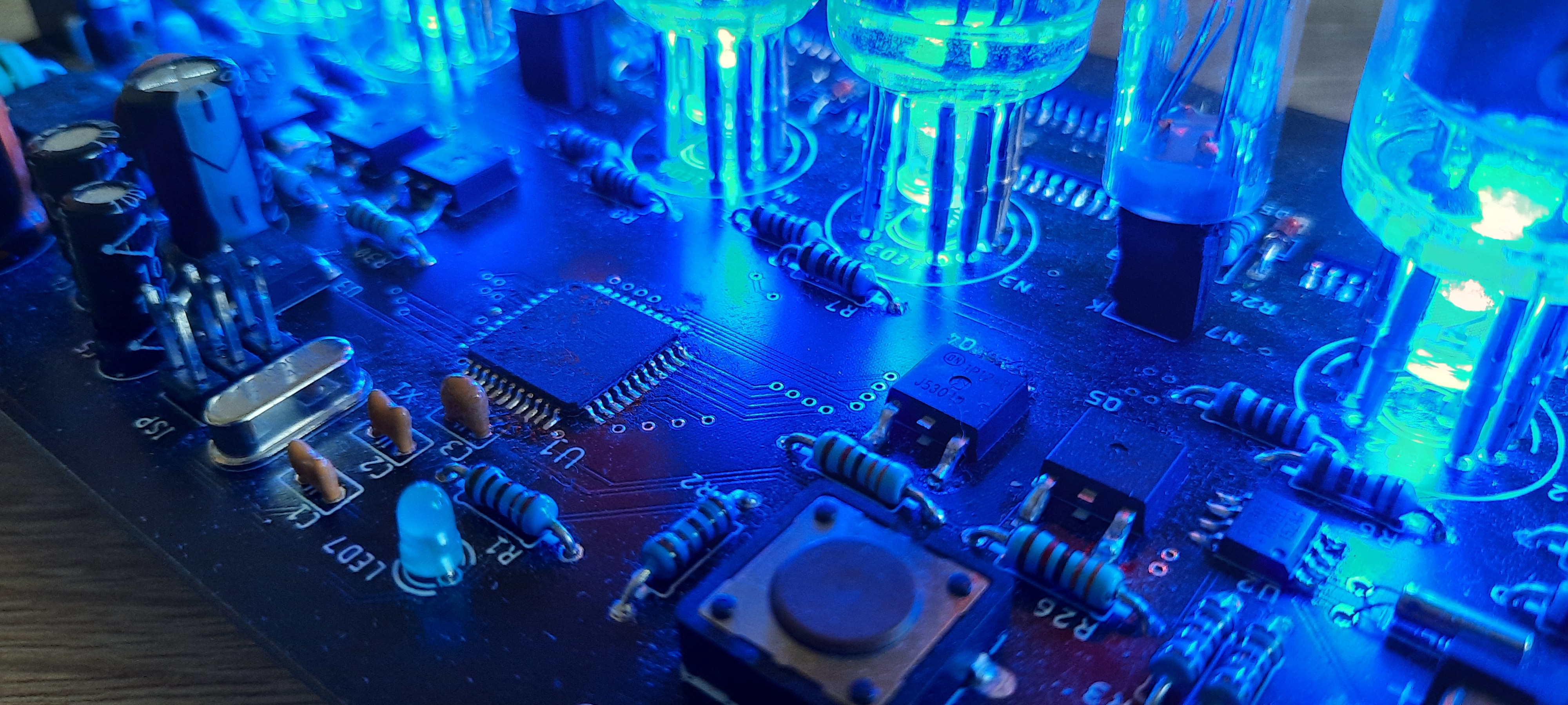
As mentioned earlier, the idea was to control the whole clock from an ATmega microcontroller. I already had some experience using embedded C on one of these from uni, so figured that it would be easiest to use one again. I selected the ATmega32 variant, partly because it had a large number of I/O pins (32) compared to the ATmega328 variants that Arduinos use, but also because it was one of the only chips I could find in stock online! I picked up 8 of them in case I wanted to use them in other projects, and the chip shortage didn’t alleviate soon. I chose the TQFP44 package simply because I thought it looked cooler than a DIP40 package.
It was surprisingly easy to integrate the ATmega32 into my schematic. The only additional components I needed to add around it were some decoupling capacitors on the supply pins, an external clock source (I went for a 12MHz crystal), and a reset button. With two of the I/O pins dedicated to I2C communication, three dedicated to SPI and ISCP communication, as well as one to control the LEDs, and one to control each colon digit separator, I had 24 I/O pins left to control the nixie digits.
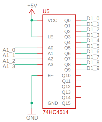
However, each nixie tube has 10 separate cathodes, that all need to be controlled. With 6 tubes, it seems I need 60 I/O pins. Not to worry! We can use decoders to drastically reduce the number of I/O pins necessary. A decoder is a type of digital component that takes a binary number as an input, to select a particular output. This means that n inputs (the binary number), can control 2n outputs. I ordered some 74HC4514 latched decoders (4-16). They take a four bit binary number as an input, and this selects one of 16 outputs. For example, applying an input of “0101” would result in Q5 being turned on, as 0101 is 5 in binary. These chips also have a latch function, where you can lock the output in a certain state, but we are not going to be using that feature. Therefore I have pulled the latch enable pin to the supply voltage, as well as pulling the chip enable pin (active low) to ground.
In the schematic to the right, the nets labelled “A1_x” refer the connections made to the microcontroller, while the nets labelled “D1_x” refer to the outputs of the decoder, which are connected to the inputs of the ULN2003A Darlington array drivers.
Using one decoder per tube simplifies things, as now we simply have to send the decoder the number that we want to appear on the tube, in binary. I connected the decoders to the microcontroller I/O pins on the same port, and in order, if it was possible. This will mean that during programming, I will be able to simply set a number to the relevant I/O pins, and the respective tube will display that number! Also, we have now reduced the number of control signals per tube down from 10 to 4. Therefore, with 6 tubes, we now only need 4*6=24 I/O pins! Exactly the number we have available! How handy.
Real Time Clock with I2C
The clock, being a clock, needed some way to keep track of the time. I decided that the easiest way to do this was to use a Real-Time Clock (RTC). This is a type of chip that can keep track of time. I selected the very common DS1307 RTC, and used a 32.768kHz external crystal for timing purposes, as well as a 3V coin cell battery as a backup power source, so that the RTC can keep track of time even when the clock is switched off.
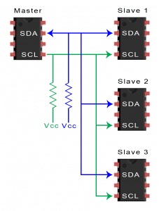
The DS1307 can communicate with microcontrollers over the I2C bus. I2C is a synchronous serial communication bus developed by Philips Semiconductors, and is one of the most widely used serial communication protocols, particularly between microcontrollers and peripherals. It requires two connections, SDA (Serial Data), and SCL (Serial Clock). The clock line is used to keep communication synchronous, while data is sent over the SDA line. To start any I2C communication, you must first transmit the address of the device you wish to interface with. This allows many devices (with different addresses) to be connected to the same I2C bus and not interface with each other. Pull-up resistors are required on both the SDA and SCL lines.
Looking at the datasheet of the DS1307, it tells us everything we need to know about how to communicate with it over I2C. I will note that there exist many pre-made libraries that you can use to communicate with the DS1307, but I thought that it would be more fun to go back to basics, and to directly program the interface myself.
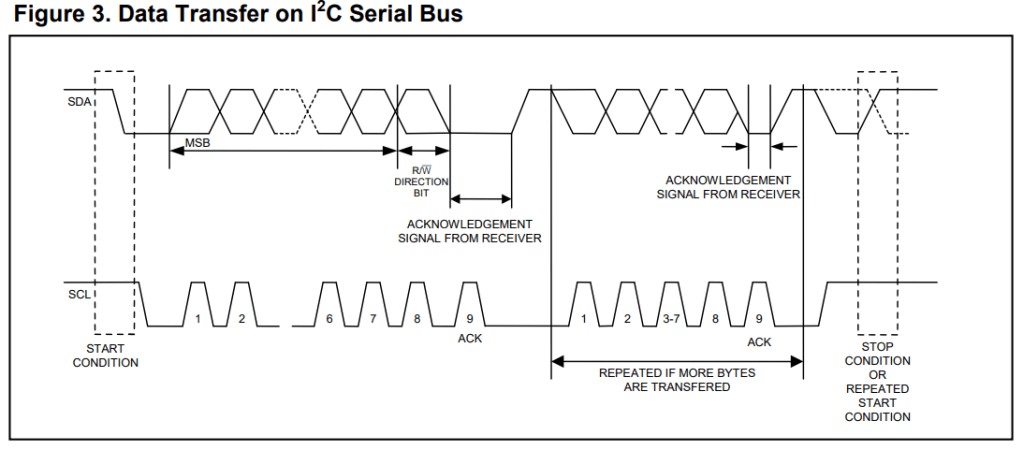
Here are some important definitions of different bus conditions that we use later (taken from the DS1307 datasheet):
- Bus not busy: Both data and clock lines remain HIGH
- START data transfer: A change in the state of the data line, from HIGH to LOW, while the clock is HIGH, defines a START condition.
- STOP data transfer: A change in the state of the data line, from LOW to HIGH, while the clock is HIGH, defines a the STOP condition.
- Data valid: The state of the data line represents valid data when it is stable for the duration of the HIGH period of the clock. That is to say that it should only change when the clock is LOW. There is one clock pulse per bit of data.
- Acknowledge (Ack): A receiver, when addressed is required to acknowledge after receiving each byte (8 bits). The master device should generate an extra clock pulse associated with this acknowledge bit. An acknowledgment is made by pulling the SDA line LOW so that it is stable LOW during the HIGH period of the acknowledge clock pulse.
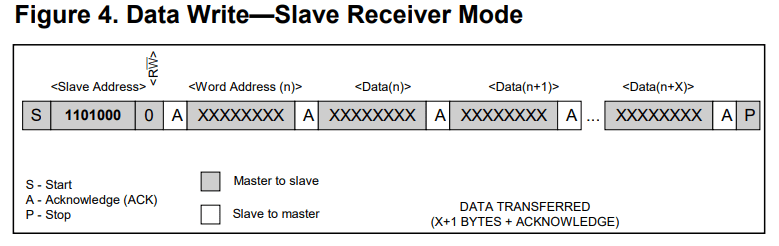
The figure above is taken directly from the DS1307 datasheet. It shows how you initialise the DS1307 in receiver/write mode. This allows you to write data to the registers of the DS1307, to set the current time, for example. First, a start condition is sent, followed by the 7-bit address of the DS1307, and the read/write bit. For write mode, a 0 is transmitted. The DS1307 then sends the acknowledgement bit, and we can proceed with writing data to its internal registers.
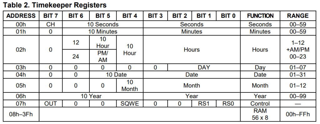
First, a “word address” is sent. This will set the register pointer on the DS1307 to the specified register. For example, a word address of “00000110” would set the pointer at register 06h. Data can then be transmitted to write to this register of the DS1307. Once the DS1307 acknowledges this, the pointer increments to the next register. Details of the internal registers are in the figure below.
Reading the time data from the DS1307 is what we will be doing during standard operation of the clock. This can be done by writing the address of the register which you need to start reading from, then sending a repeated start bit in read mode, and reading all the relevant data. When you have received all the data you want, the master should not send an acknowledge bit. This will cause the DS1307 to stop sending data, allowing the master to send the stop condition.
Power Supplies
Obviously this clock requires power supplies to function. Two supplies are needed, a low voltage power supply for the microcontroller and digital electronics, and a high voltage power supply for the nixie tubes. For the low voltage supply, 5V was selected as the voltage, because the ATmega32 microcontroller requires a voltage higher than 4.5V, ruling out 3.3V. The high voltage power supply needed to generate around 180V.
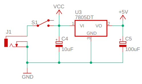
The low voltage power supply was trivial, it is simply a 7805 linear voltage regulator with capacitors on the input and output. It takes 12V as an input, and produces 5V output. The whole board is designed to run on a 12V power adapter, connected to the board via a barrel connector. The linear voltage regulator is rather inefficient, but I didn’t really care about efficiency for this application, and it was the simplest type of supply. Perhaps if I redo this project in the future, I may implement a more efficient buck converter instead.
The high voltage power supply is more interesting however. I had to find some way to generate 180V from 12V. That’s a 1500% increase in voltage! Fortunately, as is often the case, other people have had to power nixie tubes from low voltage supplies before, so I searched the internet for some inspiration. I found a design for a nixie tube power supply by someone called “Threeneuron”. They had designed a power supply based around the MC34063 Buck/Boost switching regulator.

A boost converter topology is used to generate the high voltage. Essentially, the controller chip is connected to the gate of a MOSFET (Q3), which switches current through a 100uH inductor (L1). When the MOSFET turns off, a large voltage appears across the inductor. Current flows through diode D2, charging up capacitor C9 to the high voltage. The ratio of the feedback resistors R14 and R15 determine the targeted output voltage. When compared to a 1.25V reference voltage, the ratio used produces around 180V: 1.25V / (3.32k / 3.32k + 475k) = 180.1V.
D1, Q2, and R13 form an active pulldown circuit. This allows the gate of the MOSFET to be quickly discharged when it is turned off, to minimise power loss in the MOSFET. The MC34063 regulator that I am using can only supply current, not sink it. That is to say, it can easily charge the gate of the MOSFET, but has no function to discharge it. This is simply because of the internal arrangement of the transistors. A simple solution is to just include R13, as a path to ground to discharge the gate capacitance. This active pulldown circuit however, can discharge the gate capacitance much faster than a lone resistor.
When the MOSFET is turned on, the diode is forward biased, and will have a voltage drop across it of around 0.7V. This will mean that the voltage at the base of the PNP transistor is more than that at the emitter. Remember, a PNP transistor works by allowing a small current to flow from emitter to base, which produces a large current from emitter to collector. (The emitter is the terminal with the arrow). With the base voltage higher than the emitter, no current can flow, and so that transistor does nothing. However, once the MC34063 turns off its output, the diode stops conducting, and the voltage at the base quickly becomes 0V, as it is connected to ground through R13. This allows a small current to flow from emitter to base, and thus a large current flows from emitter to collector, which quickly discharges the gate capacitance to ground.
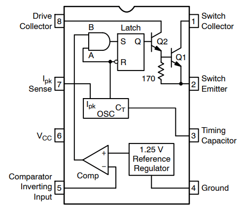
How is the regulator actually working though? Looking at the datasheet for the MC34063, we can find a simplified schematic of its internals. We can see that the feedback signal (pin 5) goes into the inverting input of a comparator, with a reference voltage of 1.25V. Therefore, when the output voltage is less than 180V, the potential divider will supply a voltage below 1.25V, and the comparator output will be high. This signal goes to an AND gate, along with the output from an internal oscillator. This will allow the latch to be set, activating the MOSFET. The oscillator later shuts off the MOSFET, by triggering the reset on the latch.
Current limiting is employed by this chip as well. the voltage drop across an external current sense resistor is monitored by the Ipk pin (pin 7). In the schematic above, the external sense resistor has a value of 0.25Ω (parallel combination). The oscillator is designed to provide an additional current path to charge the timing capacitor when the voltage drop reaches 330mV. This causes the latch to rapidly be reset, limiting the peak current that can flow through the inductor. In this case, 330mV is lost across R11 and R12 when 1.32A is flowing through the inductor.
For more detail, feel free to have a read of this application note for the MC34063.
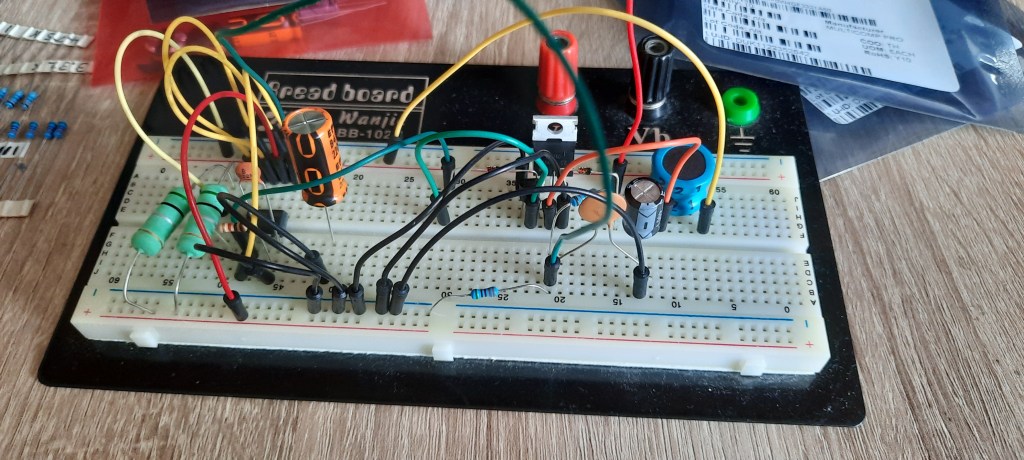
Before designing the PCB, I did build a prototype version of the PSU using a breadboard to verify that the design worked. Fortunately, it did, and I didn’t have to make any changes to it. Below you can see the prototype PSU I wired up:
PCB Design & Construction
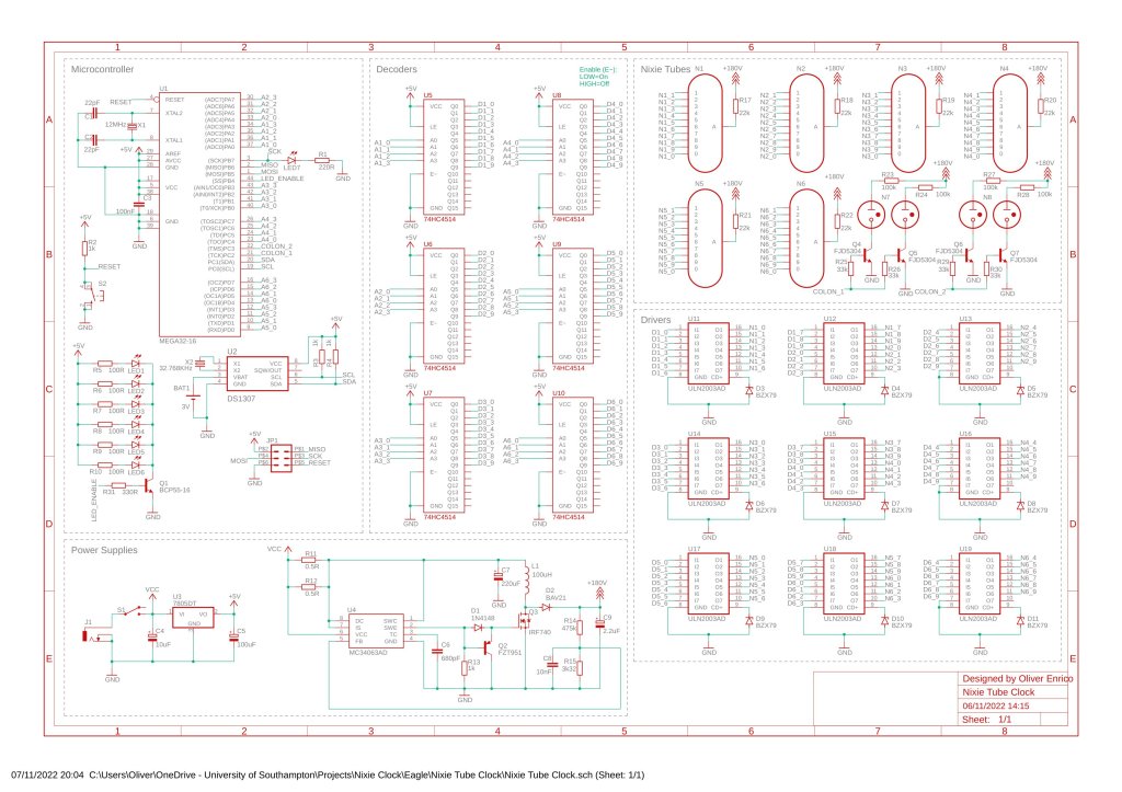
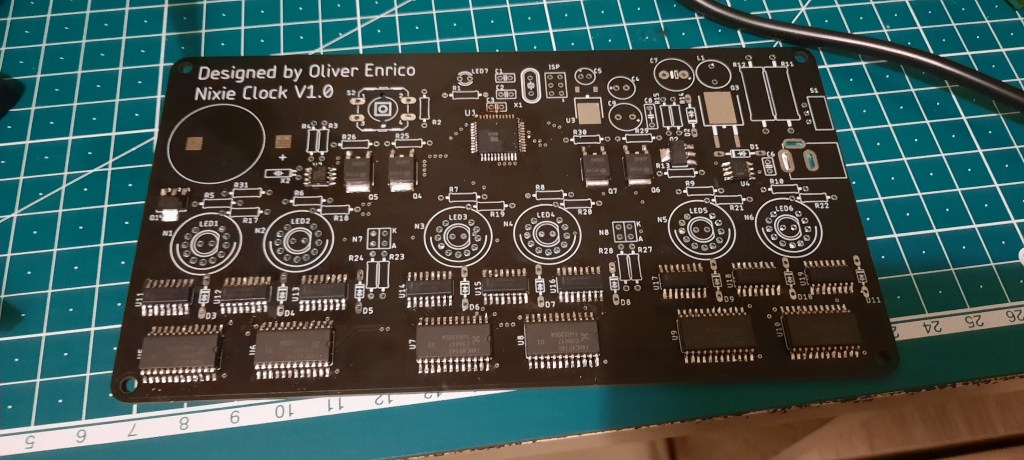
Now, all of the circuits for the nixie tube clock have been designed. Below, you can see a full schematic. A high resolution PDF version can be downloaded here. The next step is to design a PCB (printed circuit board), that all the components will be placed on.
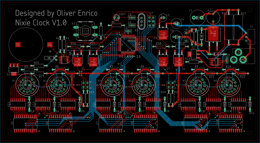
I used Autodesk Eagle to design my PCB. There’s not that much I can really say about it to be honest. It took quite a long time to get all the traces nicely organised, but overall was not too difficult to do. Below you can see the final layout for the PCB.
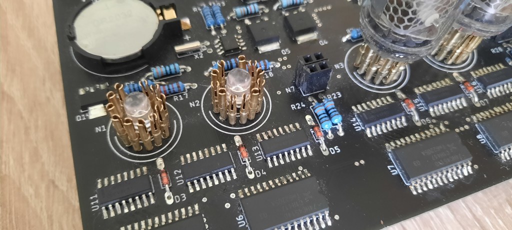
I used JLCPCB to manufacture my PCBs, the same company I have used for all my other PCB orders. They are fast, cheap, and reliable. In a little over a week, the PCBs arrived, looking very nice! I had asked for a black solder mask, as I thought it would look better for the clock. After that, it was simply a case of soldering on all the components. The only part that isn’t technically soldered on, is the nixie tubes themselves. I though it would be prudent to have them be removable, so that I could either replace them, or use them in other projects, given that they are fairly expensive. Instead, I soldered 11 little pin sockets, specifically designed for nixie tubes, in their place, and the tubes would plug into them.
Programming
With the clock itself built, the final step to getting it working was to program it. I programmed the ATmega32 microcontroller I was using with embedded C, then compiled and uploaded it using the AVRdude software.
I programmed various functions for the I2C interface with the DS1307. These are fairly standard, and set relevant bits in the I2C control registers of the ATmega32. These functions include ones that create an start and stop condition, as well as one that transmits data, one that receives and acknowledges, and one that receives without acknowledging. The function to receive without acknowledging is important, as the lack of an ack bit after a data transmission tells the DS1307 to stop sending data.
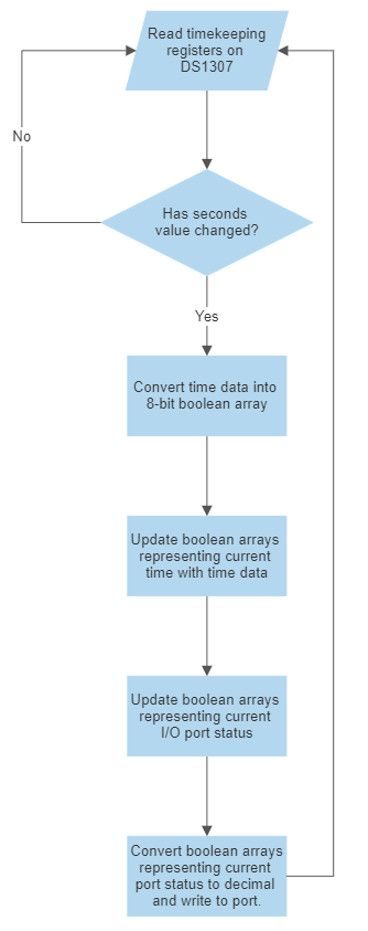
The flowchart to the right shows the basic logic as to how the clock works. The DS1307 real time clock is repeatably queried by the microcontroller, over I2C. Each time, the current time is read by the microcontroller and stored. The value of the second digit of the seconds number is compared to its previous value to determine if a second has elapsed. Once this changes, all digits on the clock update, to account for all possible time changes, up to something like 09:59:59, where all digits must change after one second.
Once we have determined that we need to update the time, the data that was read from the clock (which is stored as an unsigned 8-bit integer), is converted to an boolean array (e.g. [00100111]). There are three arrays create, one to represent the seconds, one for the minutes, and one for the hours. The first four bits in each array represent the first digit of the number, and the last four represent the second digit. For example, the binary array given above represents 0010 (2), 0111 (7), so “27”.
I then have a series of 4-bit boolean arrays that I store the current value of each nixie digit in. These get updated with the respective digit from the time data. For example, the digit representing the seconds will be updated like so: for (i=0; i<4; i++) {secondsBin[i] = secRegBin[i+4];}. Where secondsBin is the array storing the state of the nixie tube, and secRegBin is the array storing the data from the DS1307.
This is done for all the digits, and then the arrays storing the state of the nixie tubes are used to generate decimal numbers representing the current state of the nixie tubes. These numbers can then be sent to a function which will update another boolean array, which represents the current value of the microcontroller’s output port (PORTA, PORTB, etc). This is necessary, as the decoders for the nixie digits are connected to different ports, sometimes to unusual pin numbers. It is also important to not change bits on the port that we shouldn’t such as the pin controlling the LEDs, for example.
Once the PORT arrays have been updated, we then generate a decimal number from them, which we can then write directly to the port, and the digits will update.
The code also includes something I called the “poison counter”. Basically, if the nixie tubes stay displaying one digit for too long, the other cathodes can become “poisoned”. The active cathode(s) sputter material onto the inactive ones, which degrades their performance over time. A way to reduce the amount of poisoning, is to cycle through all the digits every now and then, to activate all cathodes, which will keep cleaning off the sputtered coating before it gets too thick. In my clock, I programmed this cycle to happen every 10 minutes (600 seconds).
I have linked the full program here if you are interested in having a look.
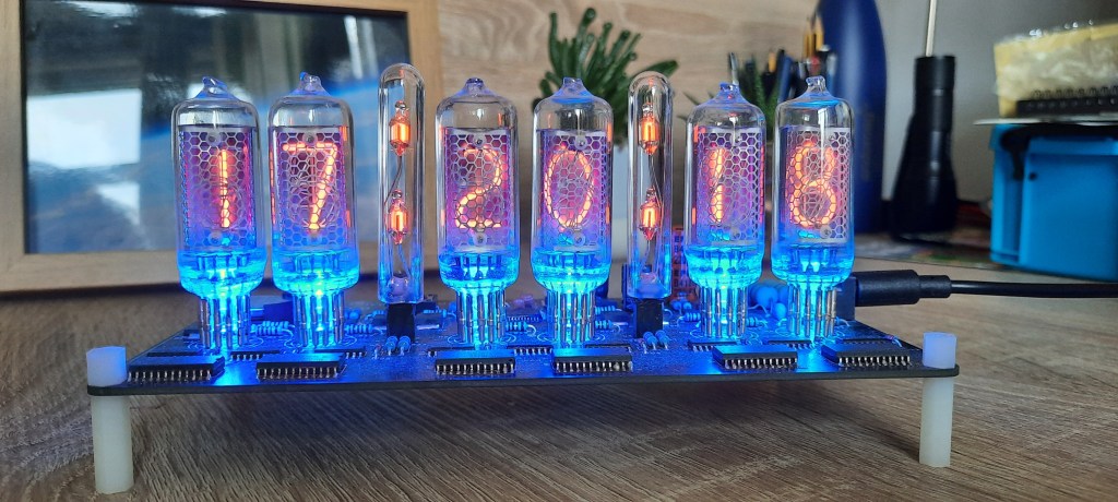
Final Result
Overall, I was very pleased the clock. I think it looks great, and I really enjoyed making it. Unfortunately, it does seem to make this high pitched-noise, much like the noise old CRT screens would make. The noise is coming from the high voltage power supply. The operational frequency is well above human hearing (100kHz), so there must be some sort of oscillation at a lower frequency happening. I’ll update this when I get around to figuring out what it is.
Update: I managed to fix the noise by changing the value of C6 from 680pF to 470pF, as well as removing one of the 0.5Ω current sense resistors, decreasing the inductor peak current to 0.66A. With less current flowing through the inductor, there is less magnetostriction, and thus the noise is no longer audible. I changed the capacitor to increase the switching frequency a bit.